Samsung Electronics (Texas) | NIST


Project Summary
The U.S. Department of Commerce awarded Samsung Austin Semiconductor, LLC, a subsidiary of Samsung Electronics (Samsung), up to $4.745 billion in direct funding under the CHIPS and Science Act to strengthen the resilience of the U.S. semiconductor supply chain, advance U.S. technology leadership, and fuel U.S. global competitiveness. Samsung – the only leading-edge semiconductor company that is a leader in both advanced memory and advanced logic technologies – is expected to invest over $37 billion dollars in the region in the coming years, and the investment would support the creation of over 15,000 jobs.
Economic and National Security Impact
The CHIPS investment would turn Samsung’s existing presence in Texas into a comprehensive ecosystem for the development and production of leading-edge, current generation, and mature node logic chips in the United States, including two new leading-edge logic fabs and an R&D fab in Taylor, as well as an expansion to the company’s existing Austin facility. It also demonstrates Samsung’s ongoing commitment to the United States, where it has been manufacturing chips since 1996. By continuing to develop the technologies of the future in the United States, Samsung is taking steps towards strengthening U.S. economic and national security and increasing the resilience of both the U.S. and global semiconductor supply chains.
The CHIPS investment would be split across multiple projects at two locations in Central Texas:
- Taylor, Texas: Construct a comprehensive advanced manufacturing ecosystem that includes both high volume leading-edge logic manufacturing and dedicated space for R&D and will transform the small municipality of Taylor into an expansive hub of leading-edge semiconductor manufacturing. This ecosystem would include two leading-edge logic foundry fabs focused on mass production of 2nm process technologies and an R&D fab dedicated to research and development of manufacturing process nodes at least several generations ahead of the current one in production. It will also include dedicated space for collaboration with equipment vendors on early-stage development of new materials and equipment. The semiconductors that are designed and manufactured in this ecosystem would serve a wide variety of end markets – from communications, automotive, and defense industries to high-performance computing and artificial intelligence.
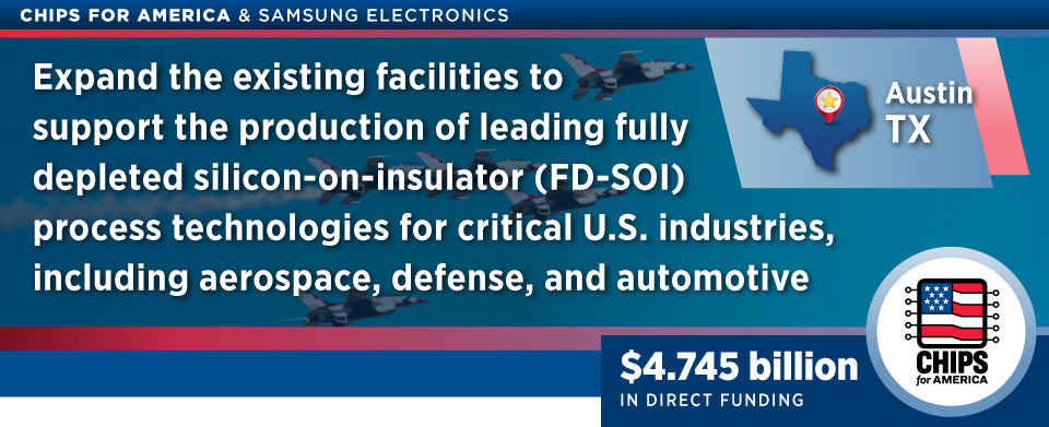
- Austin, Texas: Expand a facility that has been an economic engine for Central Texas for nearly 30 years. This investment would expand the existing facilities to support the production of leading fully depleted silicon-on-insulator (FD-SOI) process technologies for critical U.S. industries, including aerospace, defense, and automotive. This investment also includes commitments to collaborate with the U.S. Department of Defense.
Financial and Commercial Terms
As stated in the CHIPS Notice of Funding Opportunity (NOFO) for Commercial Fabrication Facilities, CHIPS for America will disburse direct funding to the company for capital expenditures spent on the projects based on the completion of construction, technology, production, and commercial milestones. The CHIPS Program Office will track the performance of each CHIPS Incentives Award via financial and programmatic reports, in accordance with the award terms and conditions.
All CHIPS funding recipients are required to adhere to restrictions pursuant to the CHIPS Act and NOFO regarding stock buybacks and national security guardrails, which limit the sharing of intellectual property. The Department and Samsung Austin Semiconductor have agreed that the company will not engage in stock buybacks for a period of five years, with specific exceptions.
Workforce, Community, and Environmental Commitments
As part of our commitment to transparency, for information on the local and community impact of this project, please download our Community Impact Report.
Samsung Project Overview |
||
|---|---|---|
Project Summary |
Recipient | Samsung Austin Semiconductor, LLC, a subsidiary of Samsung Electronics |
| Location(s) | Taylor, Texas Austin, Texas |
|
| Congressional District(s) | TX-31 & TX-35 | |
Financial Summary |
Program | CHIPS Program Office |
| Direct Funding Amount | $4.745 billion | |
| Expected Capital Expenditure | Over $37 billion | |
Workforce Summary |
Estimated Job Creation | Over 3,500 manufacturing jobs 12,000 construction jobs |
| CHIPS Workforce Funding | $45 million | |
Facility Summary |
Project Type |
2 leading-edge logic fabs, and an R&D fab Expansion of existing facility |
| Technologies |
Increased leading-edge semiconductor capacity for 2nm process technologies, and R&D focused on manufacturing nodes several generations ahead of nodes currently in production Support the production of leading fully depleted silicon-on-insulator (FD-SOI) process technologies for critical U.S. industries, including aerospace, defense, and automotive |
|
| Project Timeline | All facilities are expected to be operational by 2030 | |
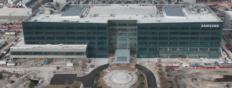
Project Photos

Credit:
Samsung


