DaMAgeCard attack targets memory directly thru SD card reader – PT SWARM
Did I ever tell you what the definition of insanity is? Insanity is doing the exact… same ******* thing… over and over again expecting… **** to change… That. Is. Crazy.
Far Cry 3
Intro
The peripheral device industry has once again sacrificed security in the name of speed. Media sizes have risen dramatically, and with them the requirements for how fast we can process media. It just takes too long to copy hundreds of gigabytes of RAW images, even with Ultra High Speed 2 (UHS-II) SD cards. And so the SD Association heard the cries of DSLR geeks, and made a move. They released SD Express1.
Our team at Positive Labs have embedded and system security as a main focus, so we’ve kept our eyes on this development. The standard was in fact published in 2018, but SD Express hasn’t gotten much traction since — until recently. Which is somewhat sad — the speed gains are enormous. But speed is not what got our attention — the way it’s achieved is. It appears that the “express” bit in the name stands for “PCI Express”, and when we hear “PCI”, we think “A-ha! Possible memory access!”.
But alas, nobody wanted to integrate SD Express into their consumer electronics until around 2022. We’re even beginning to worry — maybe this time they’ll be serious on the DMA threat front, and everything will be secure and locked up.
So while we wait for more devices to implement it (or for the industry to abandon it), we will talk about why the honorable PCI bus gets so much of our attention.
Prelude
There are many different uses for programmable electronic devices. But to make an ad hoc one each time, starting from scratch — from microchips — is economically unreasonable even with modern design tools and FPGAs. Chipmakers prefer to make “building blocks” instead, with each small controller (or whole SoC) performing as general a role as possible (but within reason). Be it for a smart speaker or a gaming PC, the “developer” (either a group of engineers or a PC enthusiast) is tasked with getting acquainted with the range of components available and picking the best ones: You pick the best general purpose processing unit, the most appropriate sensors and maybe even the cheapest memory. Then you just assemble it all, turn the result on, and smell the magic smoke feels good if it works.
But anyone who’s ever built a PC knows what really matters in the end: SPEED. It’s a complex topic that’s made up of many parts. This can again be illustrated with a PC. Of course, it matters how fast your CPU is — that’s what executes your program. But your peripheral devices matter, too. If your disk can’t read enough bytes per second, or if your WiFi card can’t receive them fast enough, you could experience stuttering even on the best CPUs. Sometimes, the speed bottleneck can be in the interface between these.
Speaking of WiFi cards, speed is not all about throughput. You also have latency and I/O wait to worry about. I/O wait is the time when your CPU can’t do anything useful while it’s waiting for data to arrive. It’s not just about the speed of your WiFi radio, but also about the way the CPU accesses the data from the WiFi card. The problem is architectural — it’s in the peripheral access model.
Let’s talk about two models: PIO and DMA. (Finally, the acronym from the header!)
In the Programmable Input/Output (PIO) model, the main processor is always the one that initiates the data exchange. It requests the data, retrieves it in some registry or whatnot, and then puts the data into the main memory. From a software developer’s point of view, this can take a few different forms. The peripheral memory can be mapped to some processor addresses, in which case it’s enough for the programmer to do some general mov instructions — this is called MMIO, or Memory Mapped I/O. In some other cases, the developer will invoke a special instruction like inb 0x8, 0xFF, which in x86-speak is “put a byte from port 0x8 into address 0xff.”2.
In both cases, the special hardware in the CPU chip will query the peripheral device, wait for the answer and put the data into the main memory. Other parts of the CPU could execute something while this hardware waits,3 but when the time comes to access memory, it’s back to sequential execution.
This could take many clock cycles, especially if there are many bytes to download4.
The Direct Memory Access (DMA) model makes the part where data is put into RAM somebody else’s problem. Now there is no reason to bother the CPU before everything is in place. So in between starting the transaction and the “ready” interrupt, the processor can execute whatever it needs. Yet a question arises — what chip or even device could do the job better than the CPU, and could be trusted with main memory?
The industry came up with an answer: a discreet5 hardware block called a DMA controller.
All it takes for the CPU to make a request to, say, copy 1 MiB from disk, is to tell the DMA controller where to put the data6.
The important part is that it is still the CPU that starts the transaction. The DMA controller is just used as an “memcpy() hardware accelerator”. And this is not a joke. Sometimes those blocks are used in microcontrollers to copy large swathes of data inside RAM. A less exotic example of this we can mention are Intel Xeon platforms.

The problem starts when an engineer gets a bright idea: “why don’t we put a DMA controller right on top of our peripheral device?”. This is known as Bus Mastering DMA.
Now, bus is a new word. When we talked about central and peripheral devices before, we evaded the question of how exactly they are connected. We should rectify this with another historical remark.
Once upon a time, humans came up with the concept of the bus. The word is derived from Latin “omnibus”, which means “for all”. A bus is an interconnect designed to send data between multiple devices in such a way that at least one device can eventually reach numerous others by the same means.
There are different types of buses, but let us mention the multidrop bus — this is when devices all share the same transmission media, and some scheme is required to decide which one is transmitting at the current time slot. This is called “arbitrage”, and “to control” the bus means being able to send data — and although close, this is not the same as “to master” the bus.
Some time after that, the microcomputer revolution happened, and humans started to make peripheral devices in the form-factor of a single circuit board (PCB) that fits inside a slot — expansion cards. Or even peripherals that are connected via a single external cable.
Then they also decided to leave behind the “each company makes their own main device and then sells rights to make peripherals with proprietary connection” approach. People created “industry standards” for almost everything. Unfortunately, it seems Apple missed the memo.
In summary, we live in a world where Industry Standard Data Transmission Buses exist, and usually when we talk about DMA, we do so with this kind of bus in mind.
Back to Bus Mastering DMA. When we put a DMA controller7 within a peripheral device, that device can now initiate memory access.
This might be useful, for example, for latency reduction in the networking stack, or when dealing with isochronous data streams. But it means the CPU is not even notified of this memory access.8
So syncing with other system components and software is not taken as a given and needs to be thought of by developers.
Which in turn makes it a source of errors and an attack vector when this is not properly considered.
A good example of this (and also coincidently of a multidrop bus) is a classic PCI bus. These buses got very popular during the times of PC/AT (thanks, IBM market analysts). It’s easy to judge the design decisions behind this bus today, but a word must be said by way of context. It was developed mainly for personal computers — devices that at the time were not exactly mobile. The main considerations were SPEED, implementation cost, and plug’n’play capabilities. Security wasn’t talked about much, and even then, what attack vector would the designers defend against? It’s an internal bus with expansion slots not accessible without opening the case. “If somebody has physical access, you have much worse problems”: this is already the realm of security guards. Who even opens their PC cases anyway? Only trained IT professionals and nerds. Worst-case scenario, we can seal the case.
If not stated otherwise, from this point on we’ll use PCI as an example bus, while trying to keep things more generic where possible.
It wasn’t worth the candles…
But what if somebody tried to exploit Bus Mastering DMA anyway? The (potential) perpetrator would need to get their hands on a device that can both be a Bus Master AND be controlled by them. This means either making the device themselves, or hacking into some existing device.
Well, not JUST some device, but one that could be made to issue proper queries. You could say “Let us dream big,” and that it’s only dangerous if the attacker can perform arbitrary reads and writes. But we could argue that DoS attacks are possible with limited writes, and info leaks are possible with limited reads. And yes, there are examples of devices on some buses that are limited in their capabilities even without additional security measures on the bus side. On a level lower than firmware.9
With all this standardization and unification, device development got less expensive, of course… But it still remains an avenue for enterprises with scarce talent and large funds, and not for one or two hooded teens on skates. Reverse engineering and hacking an existing embedded device is not only harder, but also relies upon the existence of a device that:
- can do everything the attacker wants
- has an additional interface for control/extraction10
- won’t crash the target system when attached
Acquiring this “evil” peripheral, the attacker would need to connect it to the target, and… then what? Now they could access the memory, and to gain anything they would need either find some secrets in it or mess with the execution of legitimately running programs. But here comes another round of trouble.
The target system will have an arbitrary set of programs and devices installed. If an attacker knows how to extract a key from VulnerableEncryptionApp.v1.0.0.exe, it generally does not mean they could do the same for VulnerableEncryptionApp.v1.0.1.exe or AnotherEncryptionApp.v1.exe. Scalability here approaches zero, and that’s before we mention operating systems with automatic updates! (Or custom-built kernels…)
Now the next bit of trouble is somewhat related — there is no universal memory map. The attacker would need to find out what program uses what address. And writing to (and sometimes even reading from) particular problematic addresses could just crash the system. Most of the time, that would not be beneficial for an attack.
There is also an issue with the hotplug capability. In PCI it is optional. Maybe (just maybe) the server platforms will support it. Otherwise, this means the target would need to be rebooted, which drastically limits the range of valid attack scenarios.
We have not mentioned any actual security measures yet.
…and nobody wanted to play piquet
The design of the PCI bus was adequate for its time and intentions.
Every PC in the office was closed and sometimes sealed. Hackers had their sights on “new” network access technology, which had started to become very popular. And those unhappy few who were limited to the physical access approach focused on easier attack vectors, like keyloggers. And even beyond that, there were a lot of low-hanging fruits that made DMA attacks unnecessary. Especially if you had to reboot the target. The lack of encryption and platform configuration controls meant that it was just easier to plug the disk into a controlled system and do whatever. Even if your target had encryption, in almost all cases, the proper chain of trust wouldn’t be established.
DMA attacks were left to academia11 and (probably) very rich APTs.
So nobody bothered to worry about security.
The first omen — CardBus
A few years after that, laptops started to become popular. By contrast to today, it was considered cool to have a lot of upgrade options and ports to connect peripheral devices. As a result, the PC Card was born. The typical PC Card was a network controller. It had one DMA controller on the bus and no Bus Mastering.
But then, in 1995, a new PC Card standard was released. PCMCIA 5.0, aka CardBus, was based on connecting to a PCI bus via a bridge. Of course, it now had the ability to access memory at will.
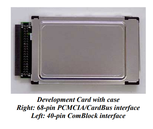
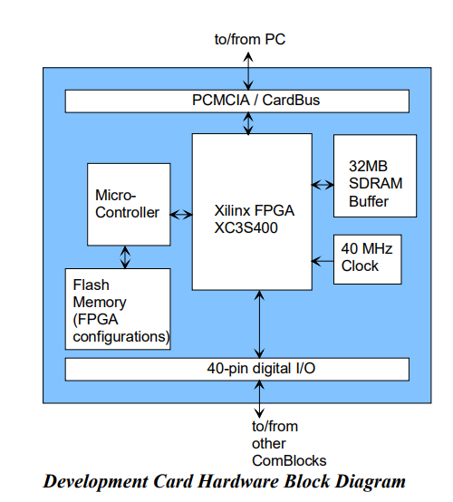
These were the first devices that both had DMA Bus Mastering and that could be plugged into a PC without disassembly. But it looks like the complexity of making one saved the public from attacks. The first mentions of CardBus being used in this way date to 2009. Researchers used the ComBlock COM-1300-C FPGA development board on CardBus to make a programmable (in assembly) attack device. It was an unstable proof of concept, with erroneous PCI implementation that crashed the target on insertion as many times as it worked.

Still, it worked… But while CardBus was early to the party in 1995, it was almost unused by 2009.
Catching fire — IEEE1394
Remember how Apple and Sony never got the memo about industry standards? In the late ’90s they teamed up to create their own competitor to the hot new USB thing (which was yet to learn of Bus Mastering). They weren’t interested in expansion cards and puny network connectors. They wanted to hit the normal people market: audio and video tech. Just like today, in 2001, the size of media files was too big to be comfortably transferred by regular methods.
Probably more important than camcorders was the release of the iPod. And this device’s big HDD would take ages to sync over USB.
So they made iLink, aka FireWire, aka — ironically — IEEE1394. It was pretty fast, and one of the reasons for that was DMA Bus Mastering. Note: it was a distinct new bus, independent from PCI! PowerMac G4, for example, came with both FireWire and PCI, and they were not interconnected themselves, but put onto a “system controller” separately. But in G5 (and in non-Apple computers) the connection uses a bridge. But this was not something inherited from PCI but something they consciously decided they needed.
So in Berlin in December 2004, researchers demonstrated an attack against a laptop via an iPod (0wned by an iPod).
Now granted, this iPod was running Linux, and was loaded with libraries for FireWire interaction and some handy Python scripts. It was of course connected to the target via a FireWire cable. And the target’s monitor proudly displayed a deface program window (it’s said they also went to 3C with it and demonstrated the same on a PowerBook, but no images were found).
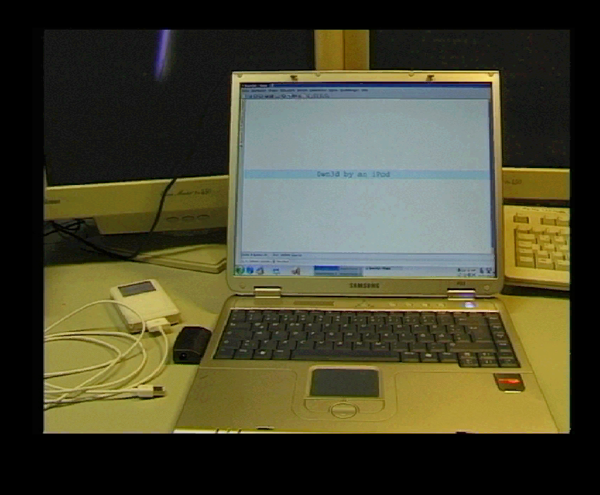
Now THIS (probably) made the public nervous. And (possibly) whispers filled the conference room: “turn it off in the firmware settings”, “put some glue in the port”. Apple, however, was not impressed. They flexed their small controlled ecosystem advantage, and just started to transparently map the memory visible to the FireWire controller into a separate (virtual) address space. We’ll talk about this later, but what matters now is that Apple (negligibly) lost in speed, but continued to use FireWire.
It runs in the family
History continued its march forward, and PCIe came to replace PCI. It’s not a multidrop bus anymore — more like a tree of devices and switches connected “point-to-point” electronically. But while PCISIG changed the physical layer, they tried to keep everything compatible on the software level, so you wouldn’t have to learn how to make drivers again from scratch. And they kept Bus Mastering, too.
The interconnect became much FASTER. It was still intended only for internal usage in PCs and servers. Hotplug became a little bit more widespread, now seen not only in servers but also in occasional workstation-grade PCs. Due to the large demand from the mobile laptop market, new form-factors were developed, because the normal expansion cards were too damn big to fit.
Laptops, huh? Got new connectors? They are still under the lid behind a bunch of screws, right? PCIe is still an internal interconnect! So the threat model hasn’t changed and everything is fine.
This is the part where we could mention ExpressCard — the new CardBus, but with PCIe instead of classic PCI. But it didn’t gain much traction on the market—most things without harsh speed requirements moved to USB, and those that had them — like disks and modems — migrated under the lid with new PCIe form-factors. ExpressCard by itself was as secure as CardBus was — with security through obscurity. But it deserves a small mention due to being used in many FireWire and CardBus adapters. Creating a Frankenstein’s monster of adapter chains became a staple in DMA attacks.
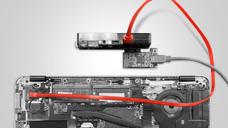
Small PCIe form-factors, called Mini-PCIe and NGFF (aka M.2) bring us closer to modern times. They are used widely today, in the desktop, laptop, and the rising single-board–computer markets. However, they inherited something very unfortunate from the PC Card — and it’s not just Bus Mastering. Both M.2 and Mini-PCIe are strictly speaking not “just another PCIe form”.
If you buy three different Mini-PCIe cards, with connectors that look nearly the same, one of them could be just a funny-looking USB device, the next one could actually connect to PCIe, and the last one could actually be an mSATA. What’s worse, take three different notebooks with a Mini-PCIe slot — they could all support just one of these. Oh, and did you know the different notebooks could actually have almost the same part numbers and look identical and only differ in model year or in some obscure serial number digit? HP surely did know.
Almost the same comes round again with the M.2 format, but with one exception—this time the connector has mechanical keys on it to differentiate capabilities. So you could — hypothetically — understand what a slot is capable of just by looking at it. In practice there are numerous nuances, like the A-E key which still can be USB-only or can connect very special PCIe Root Complex Integrated devices.
And when these new form-factors are used in the right way, they don’t give anything new to the attacker. Well except the need for another adapter, that is. They connect to the same PCIe bus that the “full” cards connect to.
Hackers want to go fast, too
Maybe this was the mindset of the Intel and Apple engineers when they started development of the Thunderbolt bus, which hit the mass market in 2011. Until its third iteration, it was mostly used exclusively to connect Mac peripherals, but then even regular Intel-platform laptops started to be given one.12
The details of its low-level implementation can be discussed at length: signal transcoding, a very complex controller, optical fiber support, many upstream-downstream ports in the topology, etc. But in our case, it would be enough to say that the Thunderbolt allows you to connect an external PCIe device directly to the internal PCIe bus via an expensive cable.
Of course, after the FireWire fiasco, the developers would have to think hard about the security aspect…

… it was not until the second version of the bus that it was given a “whitelist” feature and “disable PCIe passthrough” switch.
Jokes aside, it made economic sense! To develop a Thunderbolt-capable device, it was not enough to just find the documentation somewhere. No Chinese manufacturer could sell you cheap controllers — Intel sold them to authorized partners only. And if nobody could connect to it without Intel’s permission, and you had to pass quality controls to get permission, it was effectively secure… right? Generally, it wasn’t a bad plan, but it had four weak spots:
- The very complex and heavily integrated Host Controller SoCs used a regular external SPI flash chip as ROM.
- Important data on this ROM, including whitelist and IDs, were stored without any signatures or encryption.
- Authorized partners made many adapters for other DMA-capable buses.
- One of the Thunderbolt’s killer features was connecting eGPU—which in most cases13 was just an adapter to an actual full PCIe slot.
In summary, if you see a non-Apple laptop and some whitelisted device like a disk on a desk, you could — without touching the laptop — clone the disk ID to your device (look up Thunderspy attack). Or even better, if you see a trusted eGPU dock, you could most likely just put anything in it and it could access the memory. OR EVEN BETTER buy the same device and hit the jackpot, with the vendor using the same ID for the whole model line. (Apple was special; more on that later.)
They tried AGAIN, and released the Thunderbolt 3, now with an additional security layer — whitelist with a cryptographic challenge. Keys were still stored unprotected in the SPI flash, but now you had to disassemble the host device to bypass it. So we are basically back to square one — not that bad.
One more thing: Thunderbolt allows the computer to boot from devices on the bus, so to just disable it while booting is a usability risk. At least some laptops starting in 2019 went YOLO and just considered anything connected at boot to be allowed once. So if you could reboot the device, a form of “evil maid” attack was still possible.
Now in the fourth revision they went the Apple way, with even more harsh certification and memory protection instead of protecting the port.
Plugging the holes
Actually, since the first classic PCI revisions, the Bus Mastering capability is an option, not a requirement. When the host enumerates the bus, it reads the peripheral devices’ PCI IDs and other info from their registers, and decides if it should enable the device at all and if it will enable Bus Mastering. But the device registries are not a trusted source — no signature is mentioned in the standard.
The present author also speculates that only a negligible amount of developers even tried to make it so their device would work with Bus Mastering prohibited. So BIOS firmware developers likely just started to allow it for any device that asked. Maybe this is the reason for the lack of a simple Setup switch for a “slower but secure” mode like we have with SPECTRE.
So, the best known way to protect from DMA attacks is IOMMU. The idea behind it is basically the same as with virtual memory — when a device asks to access memory, take the address it asks for and map it transparently somewhere else. And while we’re at it, this “mapping” could even restrict different types of access for some addresses. Simple, but we require an additional hardware unit to do this, and it wastes a lot of time. Also, the drivers (but not the device) would need to support this.
The concept of virtual memory and address mapping is probably familiar to the reader, but we will give a small refresher (so you can skip this part). The computing core model does not work directly with the “RAM cells”, as in “we don’t encode chip-row-columns in instructions”. They are abstracted as multiple “linear address spaces”, where (almost) each integer address allows access to exactly one machine character.
Among these address spaces, the main one is called “physical”. Contrary to its name, it is still not strictly mapped 1-on-1 to memory cells, but it’s close to this. It also has MMIO (we discussed this in the PIO section) and some straight programmatically-generated values.
“Virtual” address spaceS are created artificially by a special hardware core (on x86 this is called MMU). Their size does not depend on the amount of RAM installed; instead, it’s (usually) linked to the largest address the CPU can handle. Each virtual AS maps individual addresses to physical AS addresses — they can overlap and not every address is required to be mapped. And the mapping can set some addresses as read-only and such.
Usually, the CPU works in one of the virtual address spaces and regularly switches between them.
But the CPU is not the only part that can be translated in this way. The main PCIe controller issues memory access requests to the memory independently from it, and has a special address space of its own. This is (unimaginatively) called a PCI Address Space and is not exactly the same as the CPU’s physical AS! Remember Apple’s FireWire fix? They just mapped all PCI ASs to the CPU’s virtual ASs, which is basically proto-IOMMU protection. You can do that when you control the driver developers.
When an “evil” device issues a request to the pci0x10000 memory, IOMMU hardware in the system bus can translate it into phys0xFF0000 (without this, it would probably go to phys0x10000). Or just disallow this request. Now different mappings can be made for different devices, and they are configured programmatically by the CPU. This mechanism is actually pretty old and was described before any DMA attacks were known. Many different implementations exist—Intel has VT-d, aka DMA Remapping, AMD calls theirs AMD-Vi.14 Apple calls their thing DART on both x86 and ARM. Allwinner and Qualcomm have their own versions.
With the number of publications about DMA attacks rising in the ’00s and ’10s, IOMMU was widely adopted by manufacturers. Can it now be said that the most important platforms are protected and DMA attacks are again irrelevant?
Thunderclap
No.
Surprisingly, to make the complex system of electronic device security work, it’s not enough to add a hardware core. You have to do boring things, too, like think about a threat model, implement software (and hardware) in the right way, enable and configure everything properly. Also, this needs to be done through the whole manufacturing pipeline — from the CPU to the laptop itself, including firmware, drivers and OS developers. Suffice to say, it’s not a primitive task.
Until the middle of the ’10s, IOMMU was just nominally used in PCs. Only Apple really used it and whipped developers into complacency. But even they haven’t enabled it by default everywhere. And regular PCs? Let’s just say you were lucky if it was possible to enable it in BIOS Setup without reflashing the firmware. It was probably disabled by default — because of the aforementioned SPEED tax. Yes, any address translation adds latency, but when your cache is small and there are a lot of devices on the bus it feels especially bad.
But even enabling it in setup was not a security guarantee. Operating systems too either didn’t have proper support or didn’t have it enabled by default. What’s more, even if they did, they couldn’t enable it for every device — outside of the Apple orchard, most devices had years old drivers and no support for remapping. They were either knowingly configured to have 1-to-1 mapping, or failed to work. And 1-to-1 mapping adds both no security and a speed tax.
Another platform that used it properly were high-end mobile ARM devices. But they are not yet a target for DMA attacks. Yet…
In this article, we haven’t mentioned much specific DMA attack HW or SW yet, but PCILeech deserves to be talked about. It was presented in 2016 as an out-of-the-box DMA memory access solution. Based on a lucky find that the PLX Technologies USB3380 board could pretty simply be made to issue R/W requests and could be reflashed, it was a FW plus control SW combo that allowed users to jump into DMA at the measly cost of a few hundred bucks. It was possibly what made the most impact on vendors rethinking their stance. The project is still going strong, now based on cheaper FPGA boards. By the way, USB3380 is an example of the “limited capabilities” we talked about earlier — it could only request memory in addresses up to 4 GiB.
However, don’t think that you’re secure just because you enabled and configured everything properly. In 2019, a Thunderclap research paper was released. It showed that even if IOMMU is enabled and the attacker’s device lies past the proper translation layer, the attacker can still do messy things by exploiting the driver’s vulnerabilities. What vulnerabilities, you ask? Well, some drivers had driver-specific data structures in memory that are device-writable, and those structures had function pointers in them. Network adapters put packets into memory and while some could be read (hence leaking data), you could also craft and inject illegitimate ones. The hard part was to be accepted as a legitimate device by the driver, which is actually simple when you remember all the system emulation software available. The researchers took code from the QEMU project and ran it on their device.
To fix this requires driver engineers to think differently (which is ironic), but still, it is possible. What is harder to fix is IOMMU granularity. Just like the CPU’s MMU, it works not per address, but per page. There are a few available page sizes, but even the smallest one could end up too large, and a page you thought was secure to hand over to the device could still contain something… Like an execution stack, as Sony PS4 developers discovered (the hard way).
ATS and race conditions also need to be mentioned. Some devices could speed up translation by caching addresses on board — in PCIe this is called the Address Translation Service capability. I think it’s obvious how this is a free ticket for a malicious device to bypass IOMMU. And race conditions are the ol’ reliable — they’re everywhere, and the handoff between firmware and OSs is no exception.
… to say the quiet part loudly, IOMMU does not provide 100% protection.
The author would also like to mention Throwhammer attacks. He likes the idea of Remote DMA combined with DDR EMI bit flips very much and thinks it’s beautiful. Too bad it’s not really practical.
SD Express
So now we’ve finished with our history lesson, we’re going to check up on vendors and see if they’ve made SD Express secure.
Looks like they haven’t.
But let’s not get ahead of ourselves and discuss what they have done in the first place. As we discussed earlier, the speed bump is avoided by linking up the card to the PCIe bus. It sounds sane: the theoretical throughput limit on the fastest regular SD cards—UHS-III—comes close to ~600 megabytes per second, all while a single lane of an old PCIe 3.0 goes up to ~1000 megabytes per second. But there are different ways of “linking up”. SD cards use their own protocol stack, which wasn’t designed to be interoperable with a PCIe one. From the contact pads to the command flow, everything is different. And should you just make these new cards use a PCIe stack instead, no old device (including all those DSLRs) will work with them.
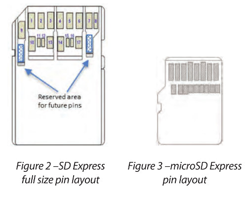
A partial SD spec is made publicly available by the SD Association and it has answers. Starting with contact pads — like UHS-II, SD Express came with an additional line of contacts on the card. Without them, there would just be too few connectors for PCIe.
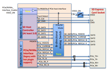
It’s implied that Express cards support two different modes of operation. The first is SDIO mode — just like a regular legacy SD card would. The second mode sees the card transition to a PCIe/NVMe device15, but even with an additional line of contacts, it isn’t enough to have an independent SD and PCIe.
The SD Express design guide points out that the PCIe differential pairs (LVDS) are connected exclusively to the host, while everything out-of-band is switched with the SDIO lines. This makes sense because LVDS — the main data conductors — are very electrically touchy and things like control signals are not.
But this could make an attack harder — what if the Host Controller doesn’t switch to PCIe mode? The spec says that the Host Controller manufacturer is free to choose which mode they try to start the connected card on, but it’s highly recommended to start with SDIO. Cards SHOULD support both options, but will they really? It would be so easy to just solder on a bunch of wires to pass our PCIe device through the SD slot, but it seems this won’t be what happens.
We decided to check some real devices. Four host devices were found on the market, and we bought all of them (taking the local SD Express market to record highs).
The first was an external card reader, which was supposed to connect to the PC via… USB3?
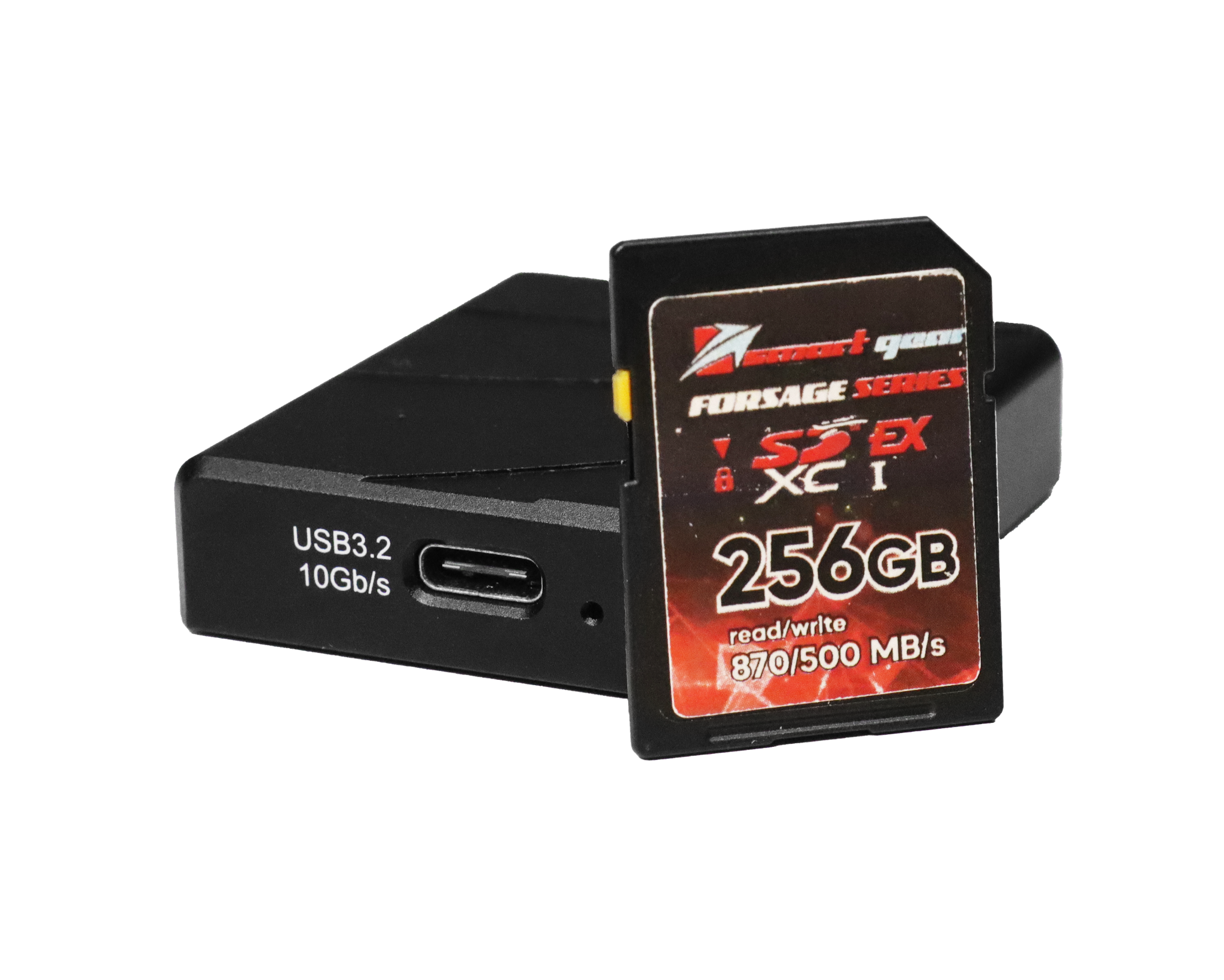
Wait a second. USB3 doesn’t do Bus Mastering. Either there’s something wrong with the device description, or there’s some hardcore multiplexing of lines going on. But the reality was less exсiting — it uses a JMicron JMS581LT host controller chip, which implements PCIe root/switch/something at least partially, and communicates with the card over PCIe. But it doesn’t pass it to the host, and communicates with the host over 10 Gib/s USB. Interesting chip overall, but not interesting as a DMA target.
The second device was a ThinkPad notebook with something that identifies itself as a “Realtek PCIe SD Card reader”. Checking the SD card port, we found additional contact pads, and we know that Realtek makes some SD Express readers, but that doesn’t mean that this is it. Booting Linux, we see the rtsx_pci driver loaded, which contains PCI passthrough code. Well, it appears this laptop contains an RTS525A chip that does not support SD Express. Unfortunately, documentation on these Realtek chips is hard to find, so we found this out by reading the driver code. If you couldn’t tell yet, this was the point we realized that the additional contact pads were the same as UHS-II.
Moving on to the third device — an MSI gaming laptop that contains an RTS5261 host controller. This is a poster chip for SD Express. Unfortunately, it has the same description string, but hey, at least the device ID differs. Installing an SD Express-capable card into it results in a very interesting metamorphosis. After the hotplug event, the PCI device tree now contains a new NVMe controller. Right at the same place where the card reader was.
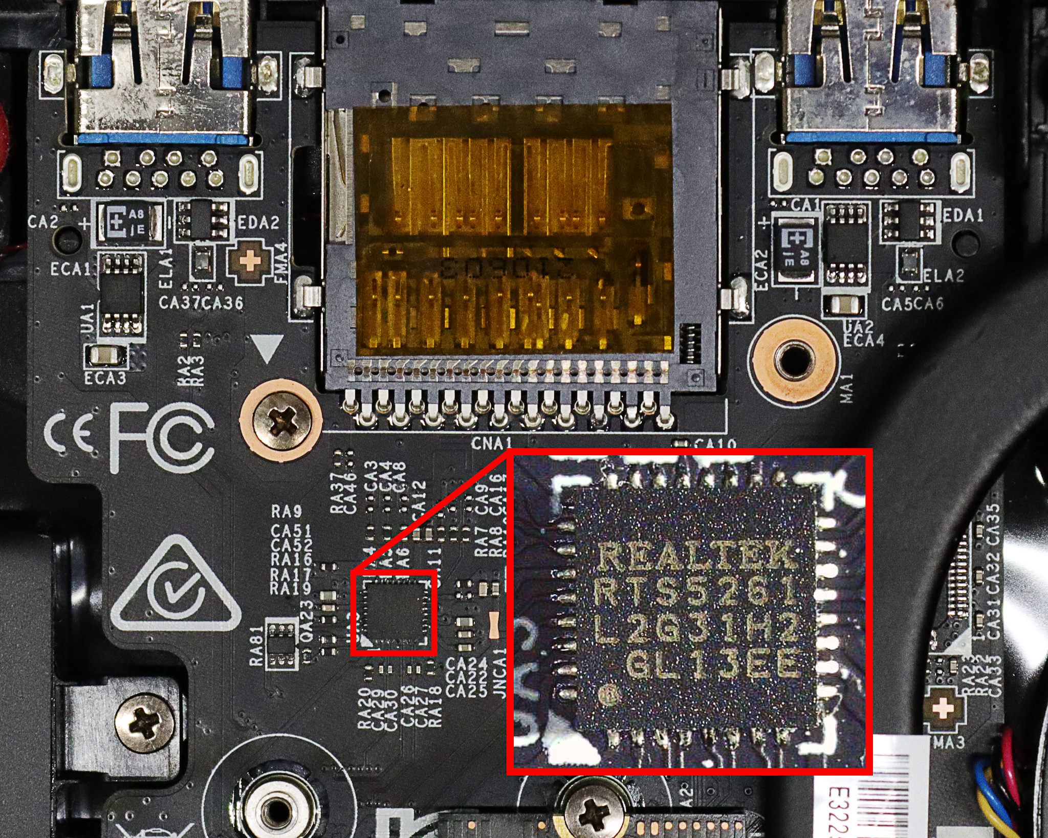
Checking the SD specs tells us that the NVMe controller should be installed onto the card itself. Hmmmmm…


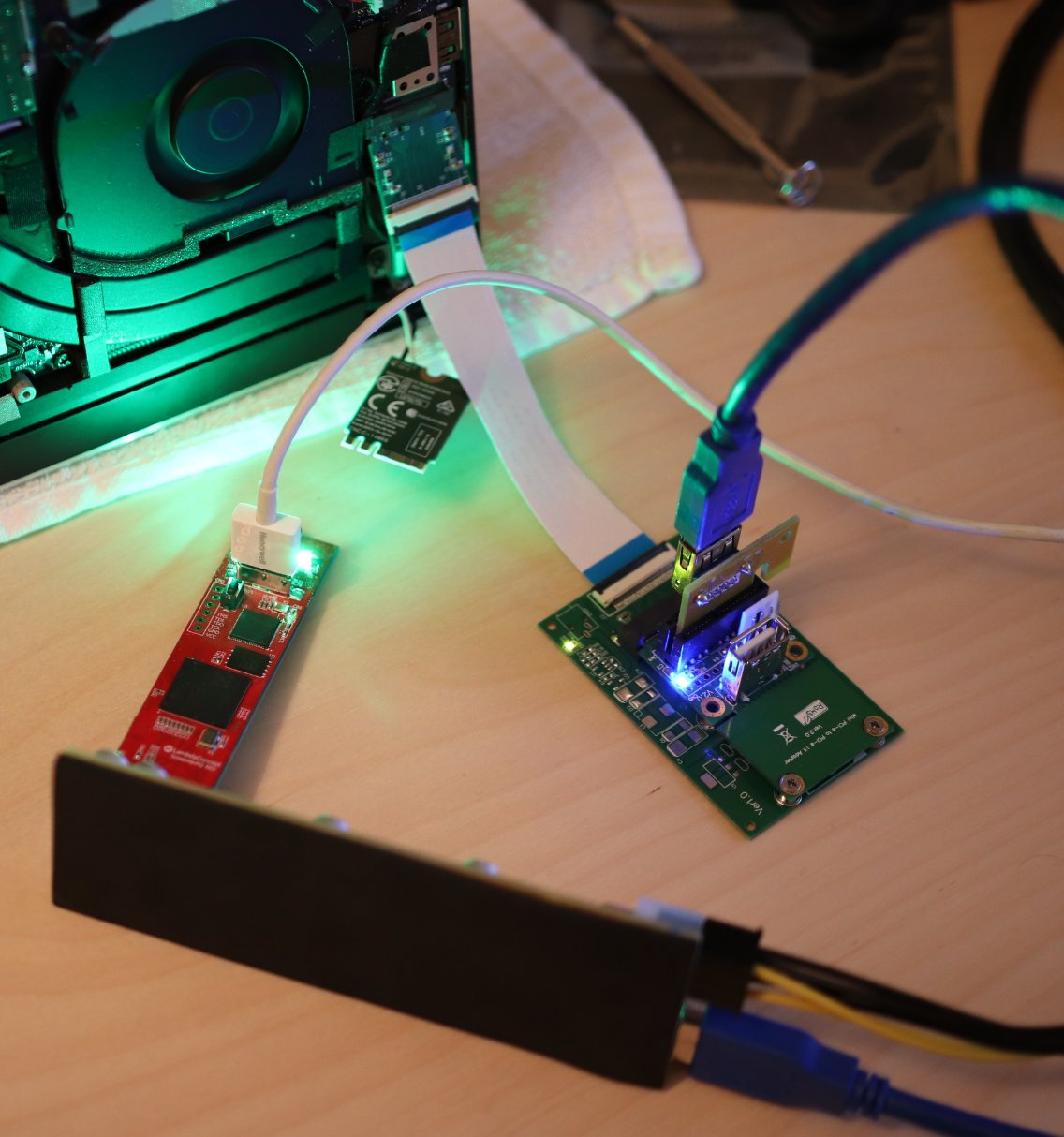
Reverse engineering and soldering the card itself was not on the list that day, so we just decided to plug in something more interesting than a card — like PCILeech. We have a lot of adapters for it, including ones we developed ourselves (a universal one! We showed it at PHDays 2). But nothing for SD.
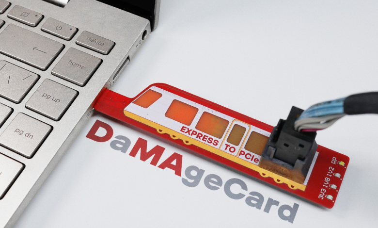
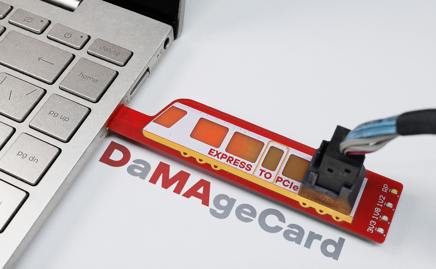
We took this as a challenge and the challenge was accepted. Soon we had made a new header bit for our universal adapter. Picture attached.
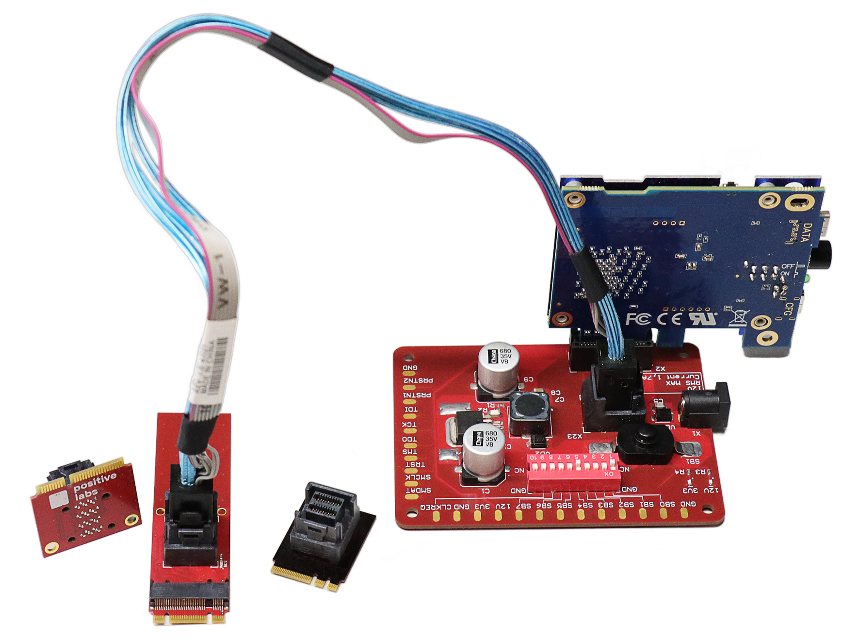
So right after the last soldering was done, we tried to use the still-warm adapter to access the memory. Nothing. PCILeech warns us of an error — we are not enumerated on the bus.
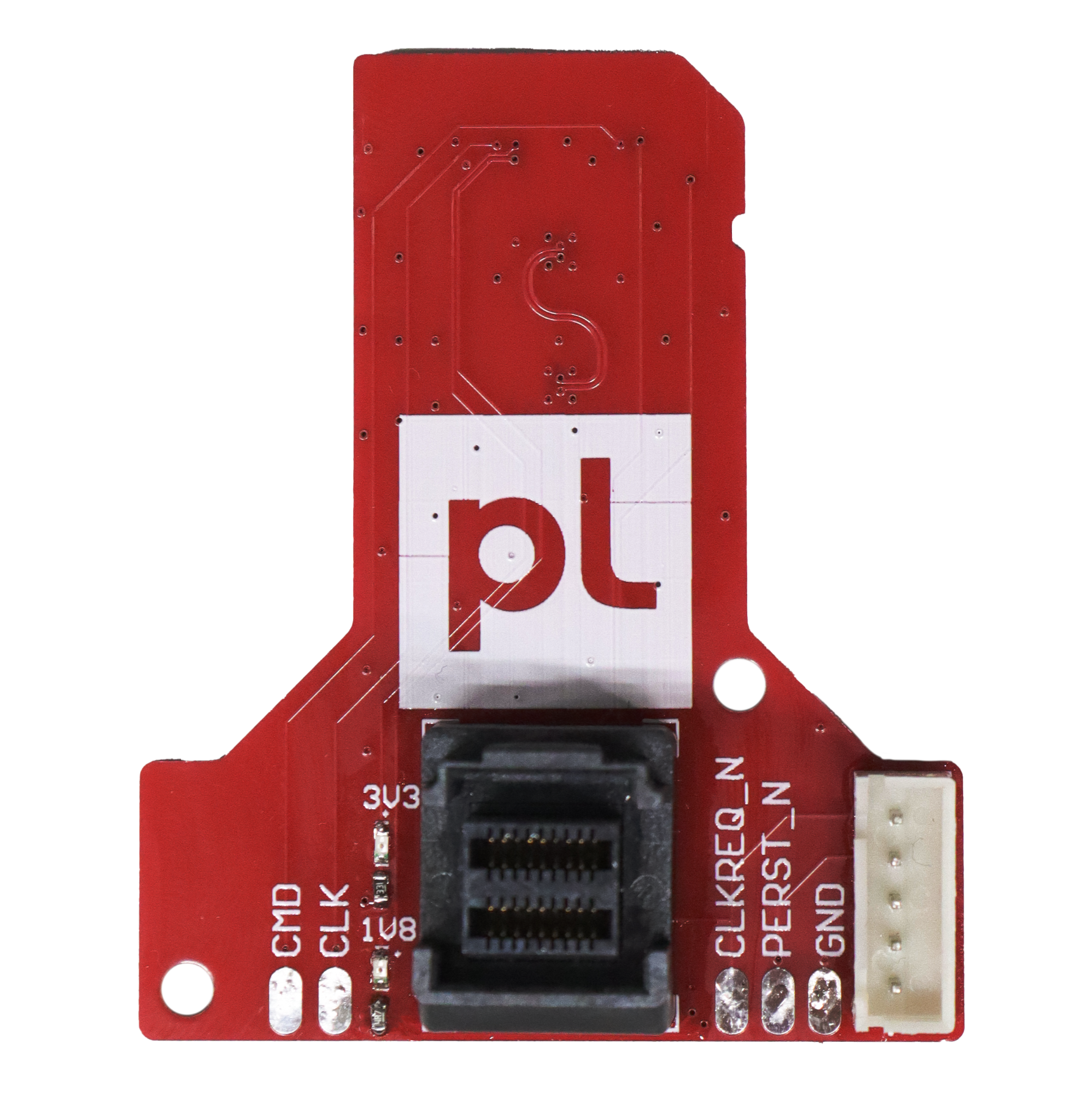
Some more thoughtful RTFM and hooking up the logic analyzer to the lines of a real card showed us that in our case the host started in SDIO mode. It sent CMD8 to ask the card about its capabilities, then started the switch to PCIe — after confirming that PCIe mode and 1V8 power was supported by the card. This complicates things… But at least nothing about encryption or credential checking was happening. We tried to solder the control lines from the real card and differential pair lines from our PCILeech.
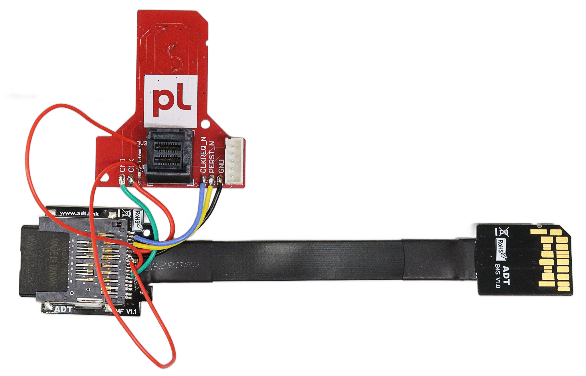
This time PCILeech could access the memory! The hotplug event fired off, the screen dimmed for a bit, and we could see an Ethernet Controller in the Device Manager in place of the card reader. The system overall wasn’t even a bit surprised or unstable.
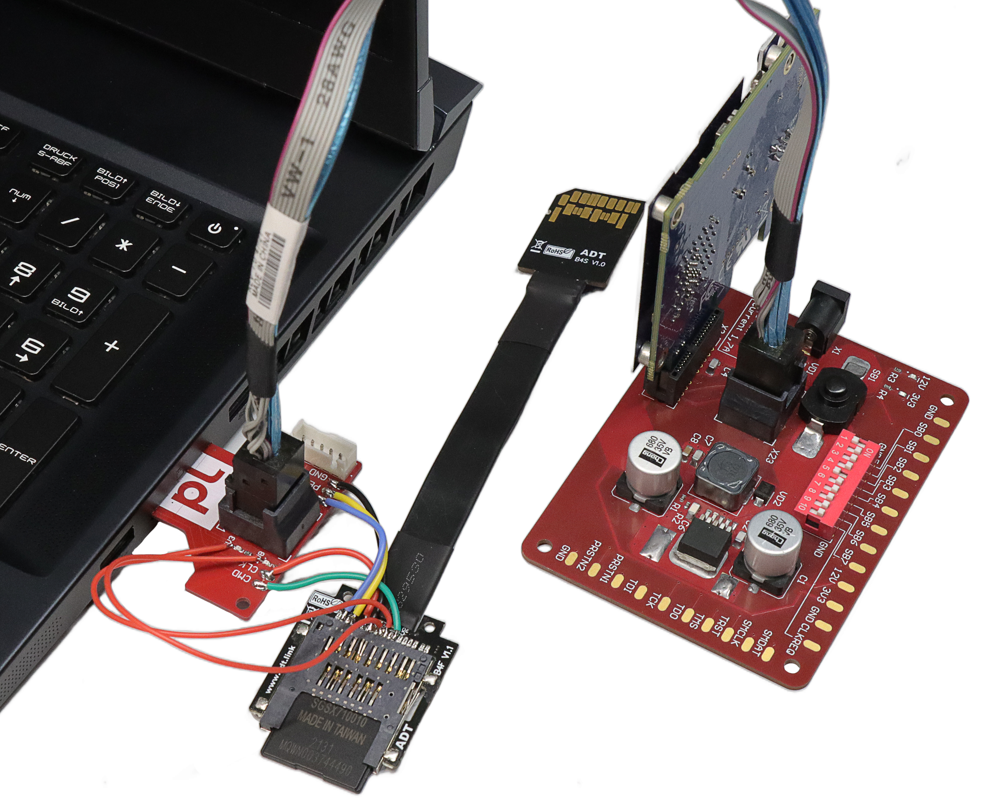
But we were limited by IOMMU, anyway. This means the developers considered this the best defensive strategy. Meanwhile, we didn’t just check with the OS running, but in UEFI too. No hotplug there, but we were able to access the memory on a different IOMMU config.


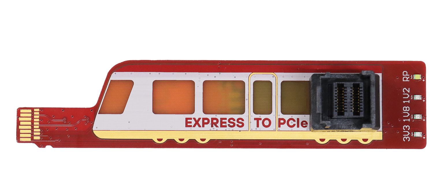
And last but not least — the AYANEO Air Plus handheld gaming console. It had microSD express — same thing, smaller form-factor. Well, we had to make another header.
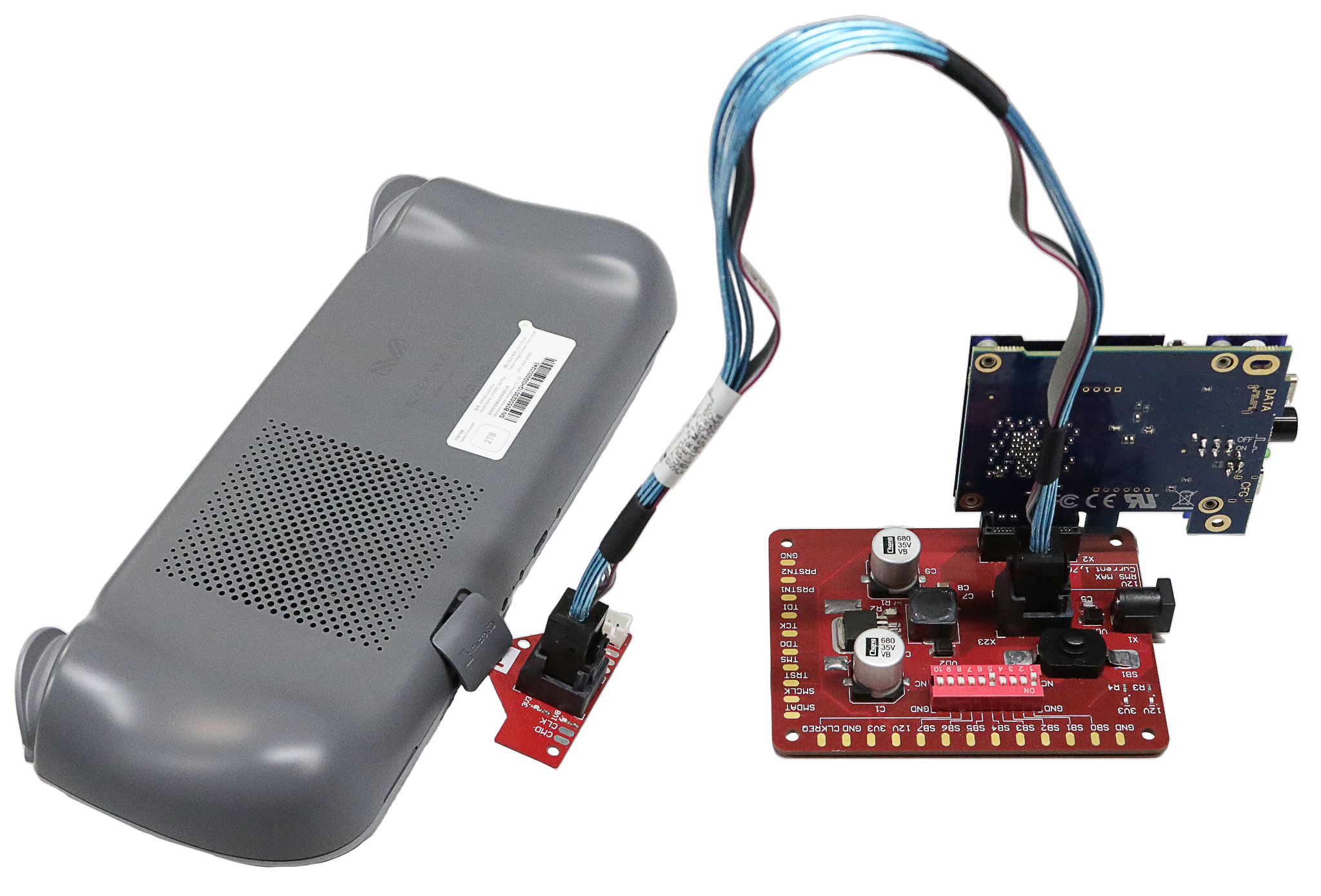
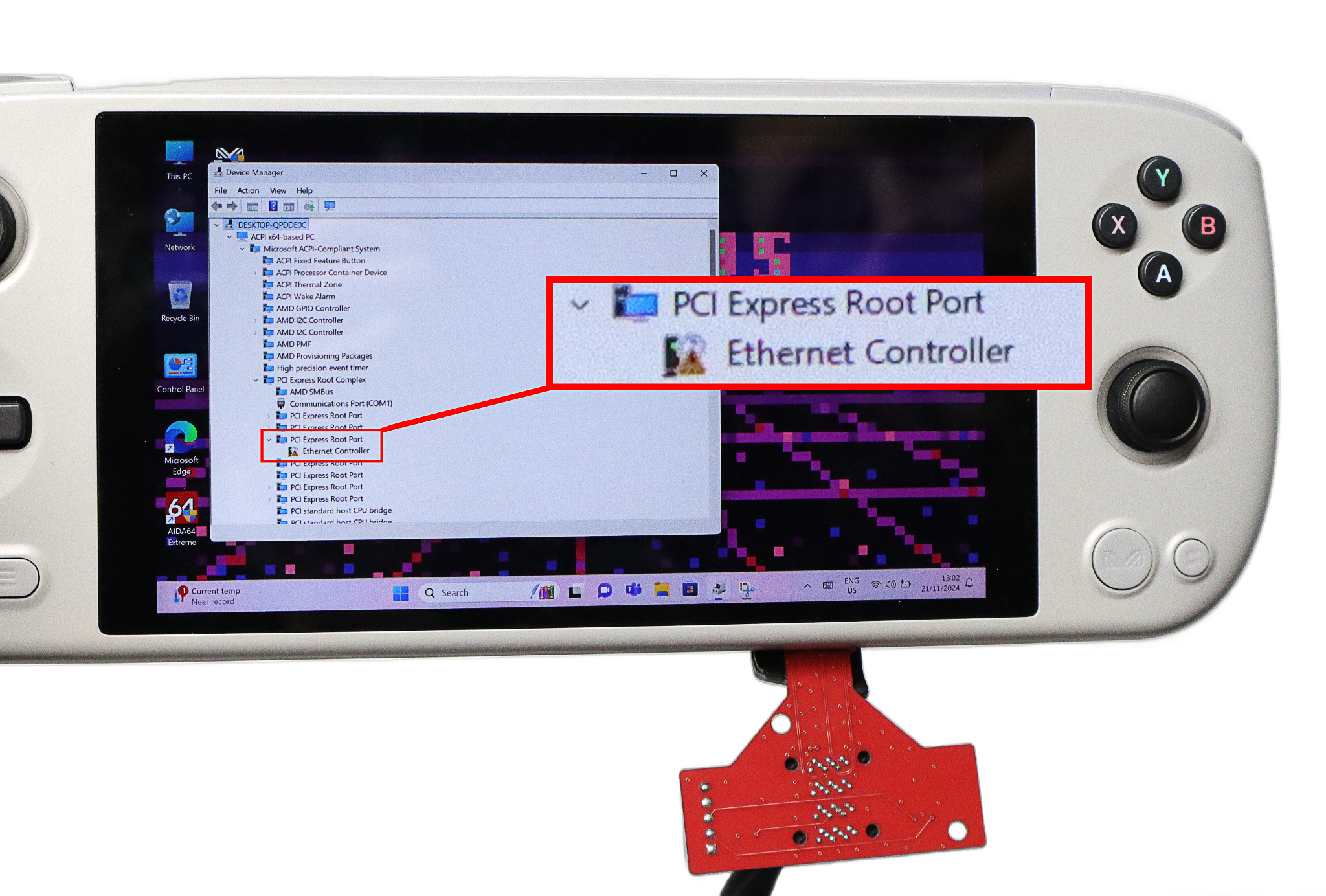
It was worth it, though—no IOMMU was set up in the console, so we could access everything. Seeing how popular different PCILeech clones are among cheaters, we’re expecting someone to release a microSD version for handheld (Hey, wanna sell us some? Strictly for research purposes ofc).
Less wires
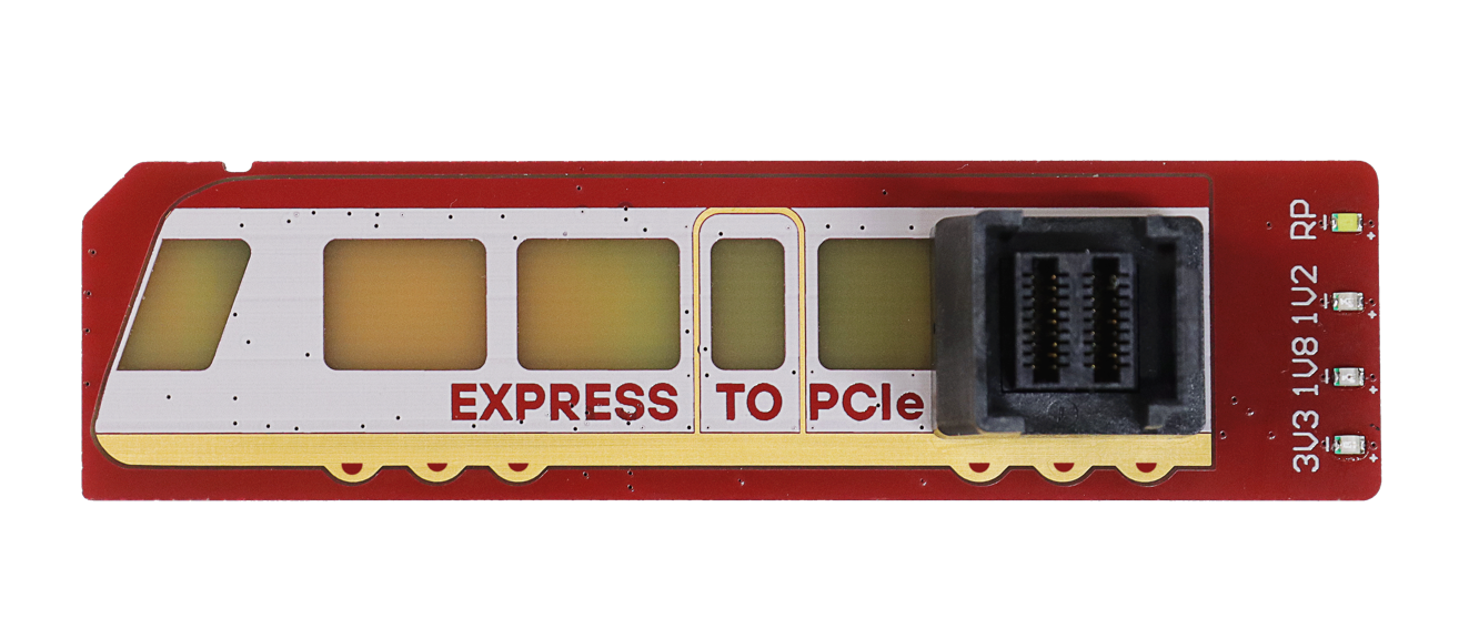
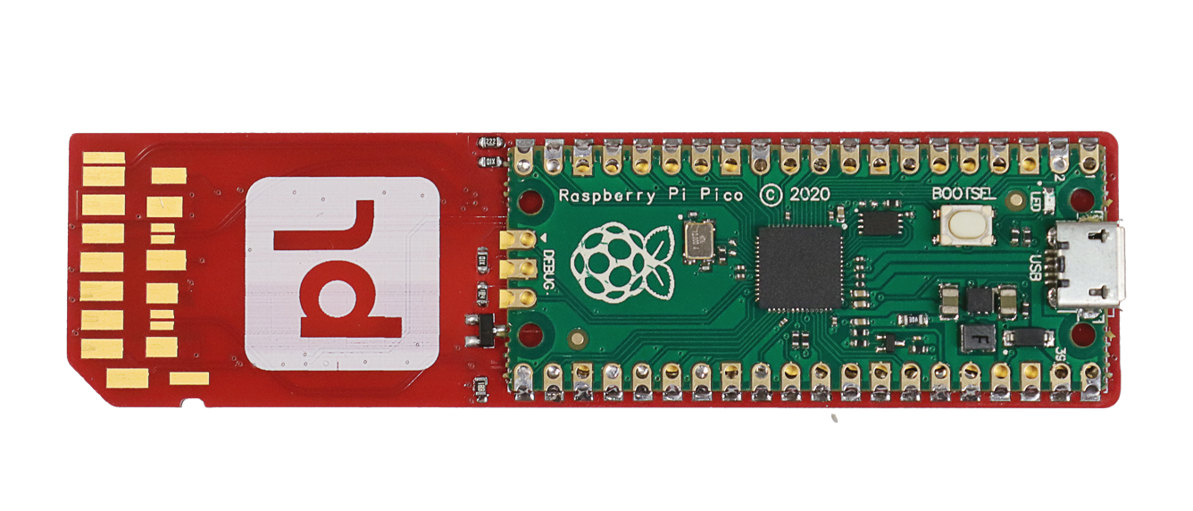
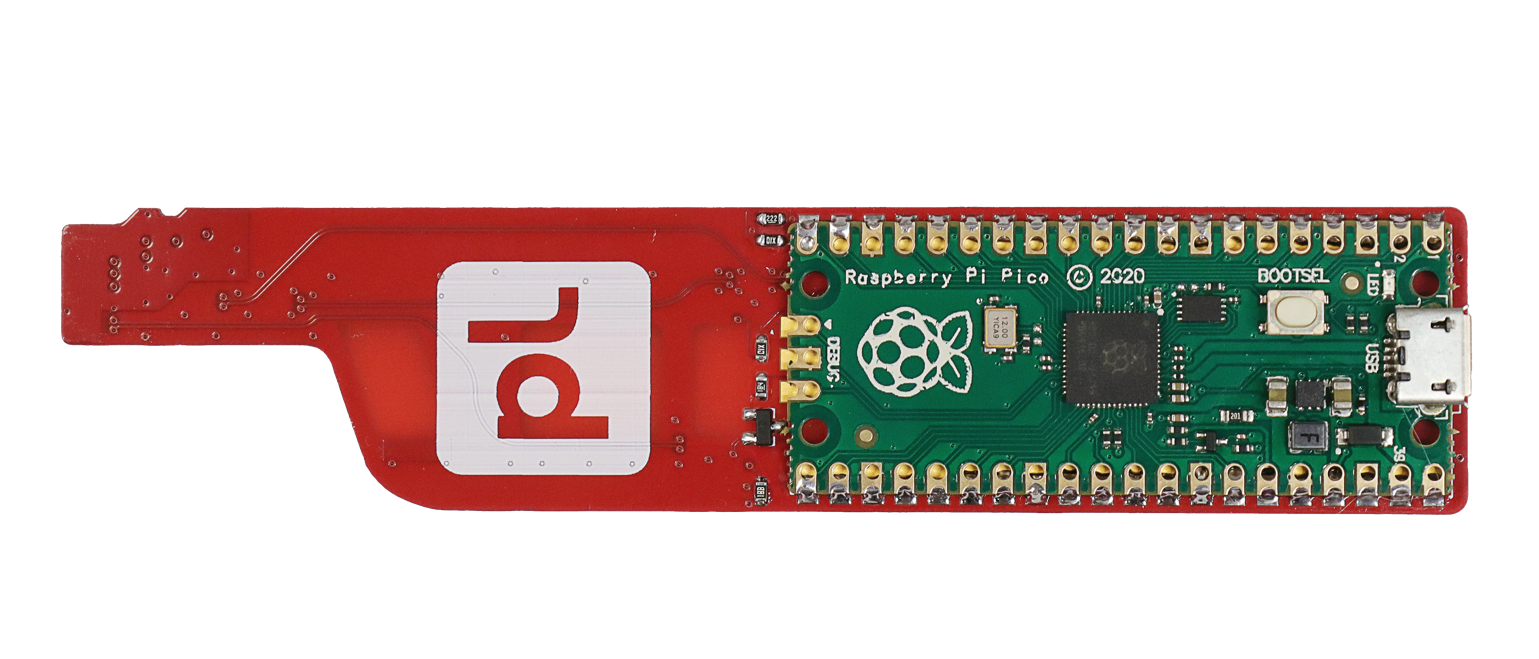
Well, our connectors work as proof of concept. Still, the need to have an original card both available AND questionably soldered onto the adapter makes it look more like a hack than a solution. Not to mention that we’re not sure that every host controller would be so kind to work with this contraption. We decided to emulate the necessary mode-switching interaction. It appears we don’t even need a hardware SD controller — a regular bit-bang approach via Pi Pico is enough, even without using Pi pIO core. (not to be confused with PIO/DMA!)
Starting with SD 7.0, two reserved bits in CMD8 are now used to encode SD Express support and 1V8 power supply support. Both our working targets required these bits to be set to logical ones.
Not just that, but after receiving the response to CMD8, the host controller pulls down the PERST# line, which is usually held up. When the host does this, the card ought to pull down CLKREQ.

The new revision of the SD Express and microSD Express adapter headings went into fabrication, now with a place for Pi Pico.
Epilogue
History has taken us full circle, and for now, DMA attacks again have a working entry point. We named this type of attack as DaMAgeCard,.
The sole difference is that 15 years ago there were no openly available tools to conduct them; not hardware, nor software.
Today, we have multiple open-source projects that provide ready-to-use solutions for extracting and analyzing memory images, bypassing authentication in modern OSs, and attacking encryption. Bleeding-edge research papers and conference talks demonstrate year after year how to bypass the sole protection solution. All the while, hundreds of thousands of devices still in use do not even have this protection enabled.
What’s next?
We think that SD Express and CFexpress16 will probably be accepted by the market — the SPEED gains are massive, and the internet is full of photographers who are happy with it.
If we end up being right, this means that the tech will trickle down from high-end gaming laptops to the mid-range segment and business workstations. Oh, and other markets too—as we see with AYANEO. For gaming consoles, hardware-based attacks are nothing new, but there are so many possible new targets: smartphones, embedded single-board systems, videocams. And other devices that need speed, but could not adapt Thunderbolt for reasons of usability, or formfactor, or licensing.
Footnotes

